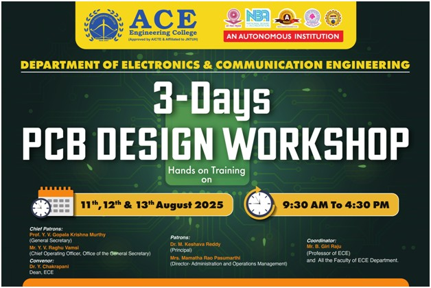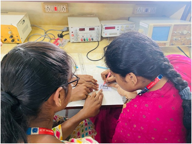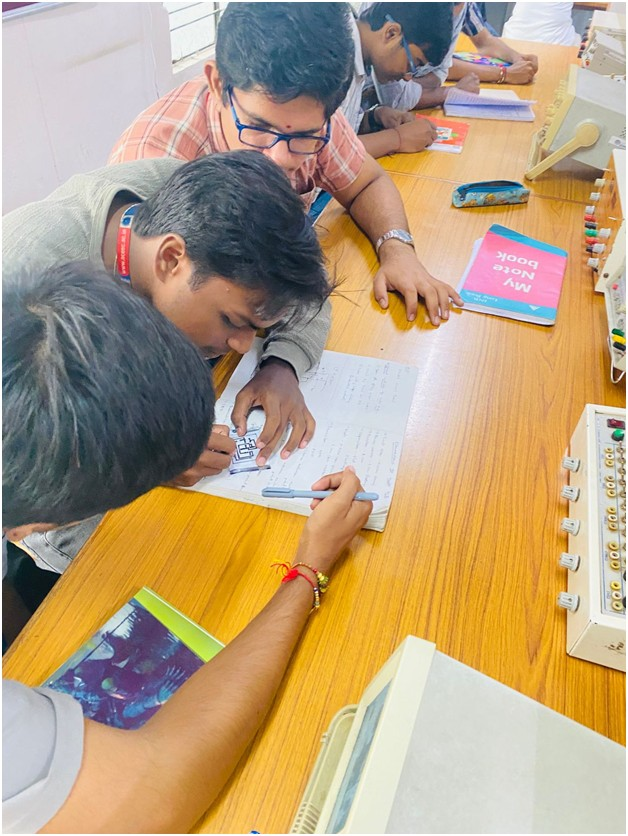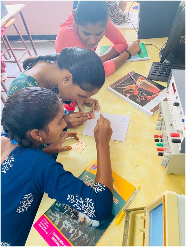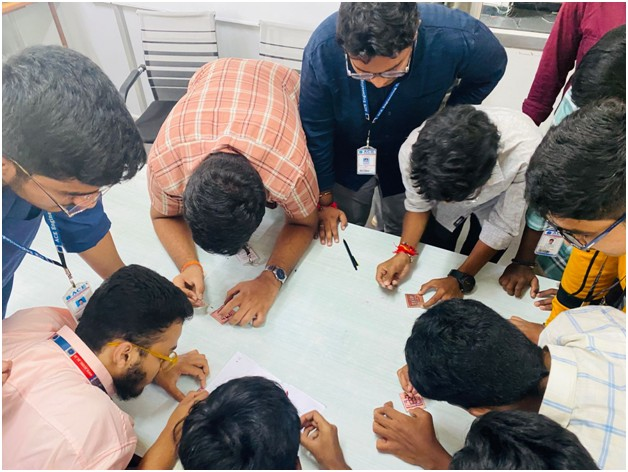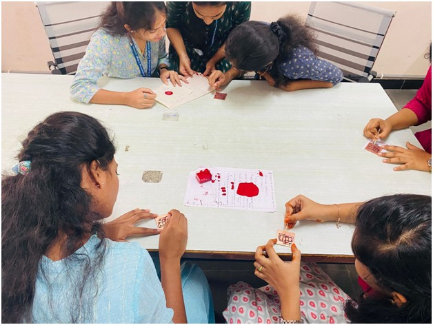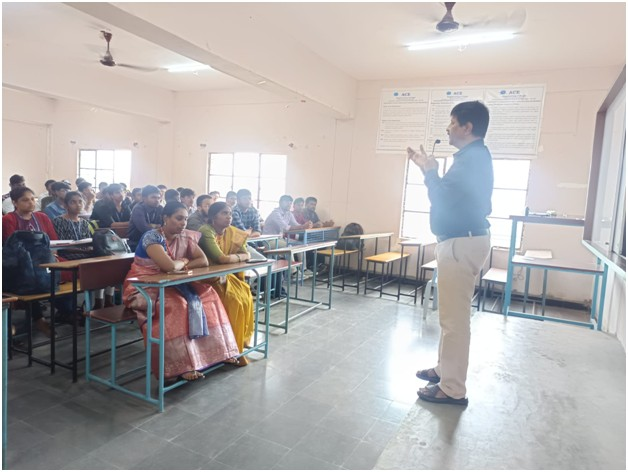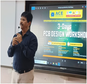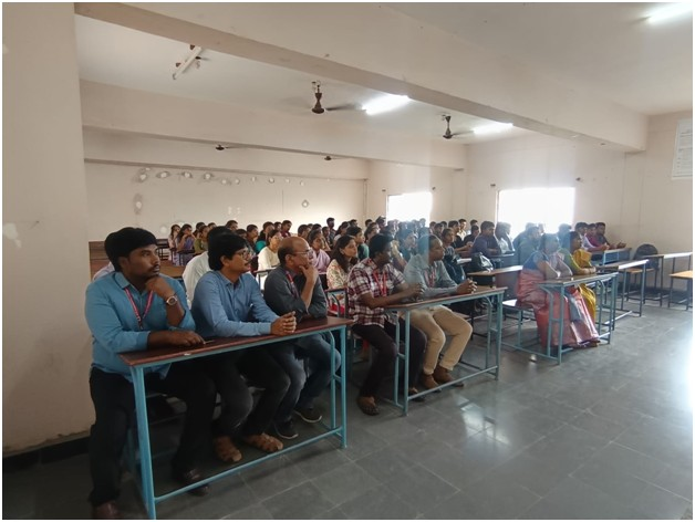
A three-day hands-on workshop on “PCB Design” was conducted by the Department of Electronics and Communication Engineering (ECE) on 11th, 12th, and 13th August 2025. The workshop provided participants with practical training in Printed Circuit Board (PCB) design, covering schematic capture, component placement, PCB layout, routing techniques, design rule checks (DRC), and PCB fabrication fundamentals. Through interactive sessions and hands-on exercises, students gained valuable practical knowledge and enhanced their circuit design and PCB development skills.
Event Gallery